| Operational Status | ● Offline | |||||||||||||||
|---|---|---|---|---|---|---|---|---|---|---|---|---|---|---|---|---|
| Description |
 The EVG 501 is used to bond 4" silicon wafers together using a combination of pressure and heat.
Patterned wafers can be pre-aligned in the EVG 620 Mask Aligner using a special fixture which facilitates precise
registration of two wafers in the aligner prior to using the EVG 501 Wafer Bonder. Once the wafers are aligned,
the fixture is moved to the bonding station.
The EVG 501 is used to bond 4" silicon wafers together using a combination of pressure and heat.
Patterned wafers can be pre-aligned in the EVG 620 Mask Aligner using a special fixture which facilitates precise
registration of two wafers in the aligner prior to using the EVG 501 Wafer Bonder. Once the wafers are aligned,
the fixture is moved to the bonding station. |
|||||||||||||||
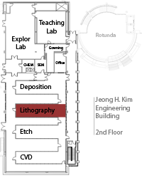
| Location | FabLab |
Photo Tunnel
|
|||||||||||||||
| Manufacturer |
EVG 501 |
|||||||||||||||
| Staff Contact |
 Jonathan Hummel Jonathan Hummeljhummel1@umd.edu 301 405-5017 |
|||||||||||||||
| Rates | UMD $75/hr External Non-profit / University $116/hr Small Commercial / MTECH $158/hr Large Commercial $220/hr No Charge $0/hr |
|||||||||||||||
| Reservations | No upcoming reservations at this time. | |||||||||||||||
| Logs |
|
|||||||||||||||
| SOPs |
|
|||||||||||||||
| Manuals | You must have lab permissions to view the manuals. Please login to view manuals or contact the lab staff to obtain permissions. |
|||||||||||||||
| Recipes | EVG Waver BondingBonder recipes.txt (3.99 KB)EVGSOP-1.pdf (570.57 KB) JOP030121 Anodic Bonding General Recipe.pdf (80.41 KB) JOP06027 Anodic Bonding Configuration.pdf (106.14 KB) JOP070214 Wafer rougness-cleaning-bond recipe spec.pdf (50.89 KB) SOP_EVG501_Sourav_12-14-03.pdf (723.03 KB) Triple-stack anodic bonding for MEMS applications_ECS Spring Meeting 2003.pdf (117.74 KB) Wafer Bonding Review.pdf (3.02 MB) |

