 |

|
 |
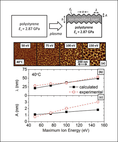
Figure 1: (a) A schematic of the highly stressed, modified layer formation and roughening that occurs simultaneously at the surface of a polystyrene film under Ar plasma exposure. Important materials and morphological properties are also shown. Below this are AFM images of the surface morphology in PS after ion bombardment at varying maximum ion energies. Also shown are calculated and experimental values of λ (b) and A (c) versus maximum ion energy of the nanoscale roughness processed at 40�C. |
|
Bobby Bruce, formerly advised by Professor Gottlieb Oehrlein, completed his Ph.D. thesis defense in early 2010. In his Ph.D. work, he was able to identify one of the root causes of uncontrolled microscopic roughening that takes place on polymer surfaces as they are contacted by plasma. Dr. Bruce will continue his work in nanoscience and technology at the IBM Research in Yorktown Heights, N.Y. He summarizes his reseach below.
The controlled patterning of polymer resists by plasma plays an essential role in the fabrication of integrated circuits and nanostructures. As the dimensions of patterned structures continue to decrease, we require an atomistic understanding underlying the morphological changes that occur during plasma-polymer interactions. In this work, we investigated how plasma surface modifications and the initial polymer structure influenced plasma etch behavior and morphological changes in polymer resists.
Using a prototypical argon discharge, we observed polymer modification by ions and vacuum ultraviolet (VUV) radiation from the plasma. A thin, highly dense modified layer was formed at the polymer surface due to ion bombardment. The ion-damaged layer acted as a barrier to further etching and significantly reduced the plasma etch rate. The thickness and physical properties of this ion-damaged layer was independent of polymer structure for the systems examined here. A relationship was observed that strongly suggests that buckling caused by ion-damaged layer formation on a polymer is the origin of roughness that develops during plasma etching. Our results indicate that with knowledge of the elastic modulus of the ion-damaged layer and the polymer being processed, plasma-induced surface roughness can be predicted and the surface morphology calculated.
In addition, we observed the absence of surface and line-edge roughness in the polymer poly(4-vinylpyridine) (P4VP) in plasma etching conditions that produced significant roughness in every other polymer structure tested. We found that in an Ar plasma, plasma VUV radiation caused crosslinking to occur below the ion-damaged layer in P4VP. For other polymers tested, VUV radiation showed no effect or enhanced chain scissioning. Our data suggest that crosslinking of P4VP by plasma VUV radiation may prevent the buckling instability that causes plasma-induced roughness by increasing the elastic modulus of the polymer region directly below the ion-damaged layer.
Overall, the present work shows that when polymers are used as resists in plasma-based pattern transfer, the effectiveness of the resist is due to the formation of a thin, dense layer at the resist surface that slows the rate of etching. However, this surface modified layer is the source of the plasma-induced roughening that leads to high roughness. Minimizing the difference in the mechanical properties between the surface modified layer and the polymer, as is achieved by VUV crosslinking in P4VP, is a possible solution to maintaining smooth surfaces during plasma etching.
May 11, 2010
|